Hanmi Semiconductor - China's antidote to EUV crisis?
- Prachurya Bharadwaj
- 2 days ago
- 1 min read

Updated: 2 days ago
The semiconductor industry is built around top-down lithography
Modern chips are manufactured by:
Growing ultra-pure silicon crystals
Slicing them into wafers
Depositing films
Patterning features through lithography
Etching and repeating hundreds of times
Every fab, supply chain, design tool, and process engineer is optimized for this approach. ASML's dominance comes from producing structures at nanometer scale reliably and repeatedly.
Interestingly, China has been investing heavily in areas that partially reduce dependence on EUV:
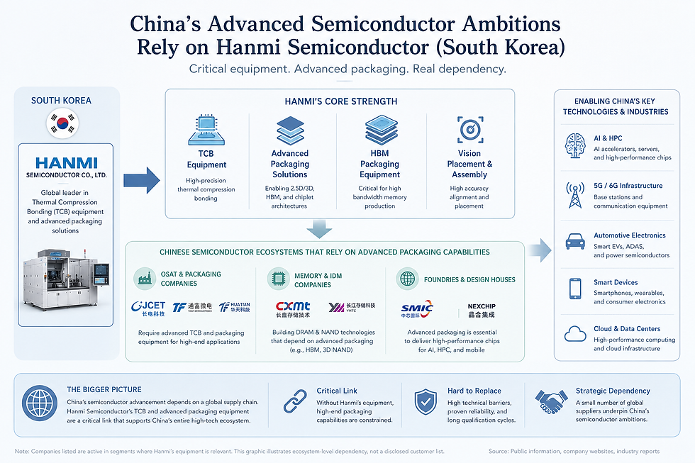
Advanced Packaging
Companies like:
Hanmi Semiconductor (Korea) - provide the packaging equipment
JCET (China), Tongfu Microelectronics, Tianshui Huatian work on packing process
show that packaging can sometimes create performance gains without needing the smallest lithographic node.
Chiplets
Instead of:
One huge monolithic die
Use:
Multiple smaller dies
Advanced interconnects
This reduces pressure on leading-edge lithography.
DUV Multipatterning
SMIC's reported 7 nm-class products are believed to rely heavily on advanced DUV techniques rather than EUV.
This is expensive but avoids the immediate EUV bottleneck.
Using these insights and several other streams of directions in the Semiconductor industry, Hanmi Semiconductor Co. Ltd. have been presented with a market strategy to prepare their product lines for the future of Semiconductor industry. To make that strategy viable, a supply chain trasnformation startegy has been suggested. Thereafter, an enterprise architecture strategy to make sure tht the vision of the executives reach each and every personnel in the organisation seamlessly.

